
What is Printed Circuit Board Testing and Why it is Important
Read Time:2 Minute, 30 Second
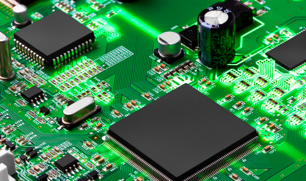
Using conductive tracks, pads, and other features etched from one or more sheet layer of copper PCB mechanically supports and electrically connects the electronic components. In PCB, some lines and pads connect various points. Signals and power are routed between the physical devices with the help of printed circuit boards.
The metal known as the solder makes the connection between the surface of the PCB and electronic components. Working with the PCB is all depend on the testing before going for the printed circuit board testing first, one must know that PCB is the foundation of any printed circuit board assembly. To meet client objectives and the performance demand, it is the greatest thrill for the engineers to nailing down the design.
Any of the designs for any device is complete when the circuit and the testing are complete from the engineer’s end. The circuit board testing method is used for the PCB for any design. The testing method by the manufacturers may vary. The tests conducted on the PCB are all among the quality control options (QC) at the time of manufacturing.
However, when the PCB is used at a high level like the government, space system, or medical sector, the testing goes high-end testing. Here the adherence to standards such as IPC 2 or 3 is required. It is not just for the high-level use of your PCB, but if you are not using it for sensitive applications, then also testing is needed. You should be confident about the quality of your board.
Visual inspection is done for the PCB construction quality check. This inspection is done through the process of manufacturing.
But here are few tests that are to be done for the high-quality testing:
• Determining the amount of strength required to peel laminate from the board peel test is done.
• Solder pot test
• Solder float test
• For the inspection of the PCB’s internal construction including layers and vias X-ray inspection is done
• AOI (automated optical inspection) is for verifying pads and trace connections. Solder quality also checks here.
• To measure the characteristic impedance time domain reflectometry (TDR) is done. Differential traces are also checked if they are matched for functional signal integrity.
• ROSE testing here all the test is done to ensure the PCB does not contain any surface debris. It also helps in detecting the excess conductive material remaining from the manufacturing process.
For the flex and rigid-flex PCB, the testing specifications are different. For the flexible printed board, IPC has published several guidelines and standards, like IPC-6013C. PCB testing is vital as in the market, and nobody can spend money on the defected or not in working condition devices.
So, from the manufacturing process to the screening, every step should be handled crucially. New technologies and changes in every sector have improved the life of living. Appliances and gadgets are all on printed circuit boards, so manufacturers must show concern and follow the testing procedure; it makes it work well.
Happy
0 %
Sad
0 %
Excited
0 %
Sleepy
0 %
Angry
0 %
Surprise
0 %


Average Rating